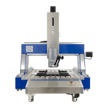
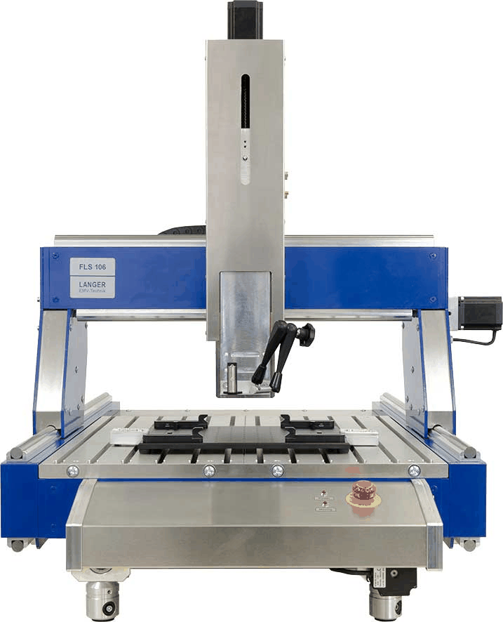
Langer FLS 106 PCB | Large-area three-axis PCB scanner
400 x 600 x 120 mm; no alpha axis | 20 um linear | USB | 110/230 V | 75 kg; 1030 x 775 x 900 mm
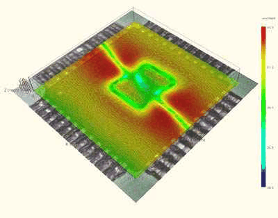
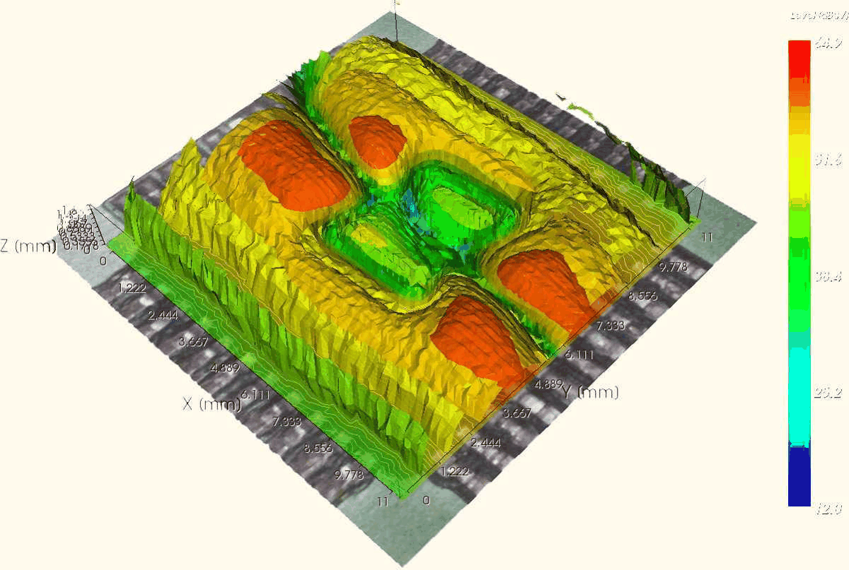
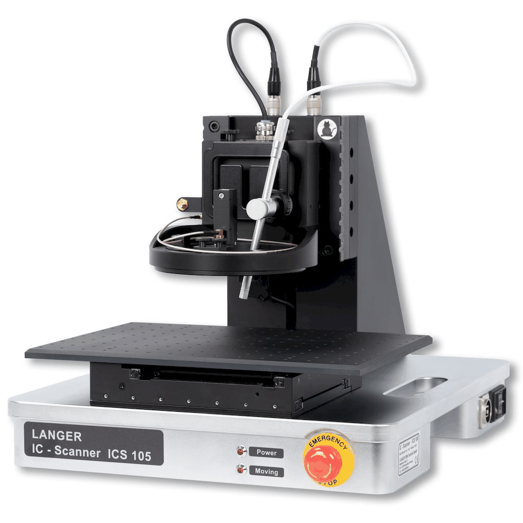
FLS 106 PCB provides automated X/Y/Z positioning over a 400 x 600 x 120 mm area for repeatable PCB near-field maps. A digital microscope camera supports optical positioning. The published collision-protection function stops downward probe movement when contact is detected; it does not replace careful setup or all protective measures.
MARKETS:
CATEGORIES:
TEST STANDARDS:
Select Options/Sizes:

FLS 106 PCB set - Datasheet
Spectrum Analyzer Compatibility
FLS 106 PCB basic set - Datasheet
CS-Scanner - Datasheet
SH 01 - Datasheet
UH DUT - Datasheet
GND 25 - Datasheet
SPECIFICATIONS
FLS 106 PCB - automated near-field scanner
FLS 106 PCB provides automated X/Y/Z positioning over a 400 x 600 x 120 mm area for repeatable PCB near-field maps. A digital microscope camera supports optical positioning. The published collision-protection function stops downward probe movement when contact is detected; it does not replace careful setup or all protective measures.
Why choose this model?
| Benefit | Engineering value |
|---|---|
| Application fit | Choose for repeatable X/Y/Z scans over assemblies without the IC model's motorized alpha rotation. |
| Reproducible positioning | Automate repeatable probe paths and document field patterns across a plane or volume. Positioning precision and field resolution remain separate specifications. |
| Probe choice | Use an E-field or H-field geometry appropriate to the suspected noise path. Microprobes resolve a smaller region than general PCB survey probes. |
| Two software packages | Full sets include ChipScan-Scanner. Basic sets omit it and target users integrating their own automation. Confirm SDK/API delivery and license requirements. |
Technical specifications - shared motion platform
| Parameter | Published specification |
|---|---|
| Supply voltage | 110 V / 230 V |
| Interface | USB |
| Max. traverse range | (400 x 600 x 120) mm |
| Min. step size | (20 x 20 x 20) um |
| Positioning speed | (20 x 25 x 10) mm/s |
| Weight | 75 kg |
| Sizes (L x W x H) | (1030 x 775 x 900) mm |
Axes: X, Y and Z; no motorized alpha rotation is specified for this model.
Full set versus Basic set - exact included items
| Photo | Included component | Full set | Basic set |
|---|---|---|---|
 |
FLS 106 PCB, 3-Axis Positioning System | 1x | 1x |
 |
CS-Scanner, ChipScan-Scanner Software / USB | 1x | Not listed |
 |
UH DUT set, Universal Holder for Langer scanner | 1x | 1x |
 |
SH 01, Probe Holder for Langer scanner | 1x | 1x |
 |
FLS DM-CAM, Digital Microscope Camera | 1x | 1x |
| safety case FLS 106, safety case for FLS 106 | 1x | 1x | |
| FLS 106 PCB acc, Accessories | 1x | 1x | |
| FLS 106 m, FLS 106 Set User Manual | 1x | 1x |
A Basic set omits ChipScan-Scanner software, but its published accessory list must also be checked. In particular, ICS 105 Basic lists GND mount instead of GND 25; the FLS 106 IC Basic list omits GND 25. Unlisted items are not assumed included. Probes and RF measurement instruments are selected separately.
Scanner accessories and configuration
| Photo | Accessory | Purpose / published specifications |
|---|---|---|
|
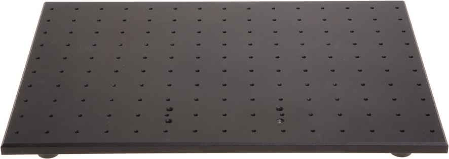
UH DUT set | Universal DUT holder set; adjustable fixation of electronic assemblies. Sizes (L x W x H): (297 x 210 x 8) mm |
|
SH 01 | Probe holder supporting the scanner collision-protection function; attachment to the rotating unit is described by the manufacturer. |
|
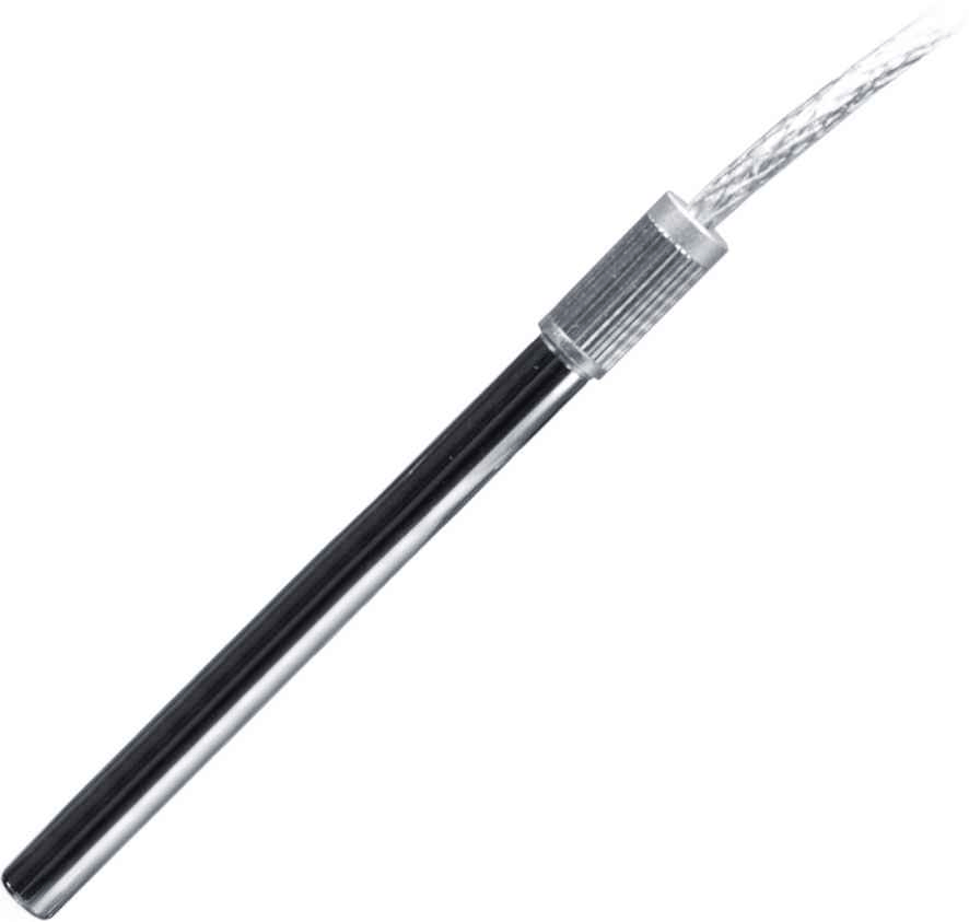
FLS DM-CAM | Digital microscope camera for the FLS 106 positioning setup. Sensor: 2.0 Megapixels CMOS; Resolution Still Image: 1600 x 1200 pixels; Image file format: BMP; Video Resolution: 1600 x 1200 pixels; Video file format: AVI; Frame Rate: 20 FPS (VGA); Focal distance: 5 mm - infinity (when focal distance is infinity, the microscope camera can't magnify); Sizes: 7.2 mm in diameter and 160 mm in length |
| safety case FLS 106 | Scanner safety enclosure; included in the listed FLS 106 full and Basic sets. | |
 |
UH DUT | Adjustable M3-screw claws secure DUT assemblies. Sizes (L x W x H): (297 x 210 x 8) mm |
 |
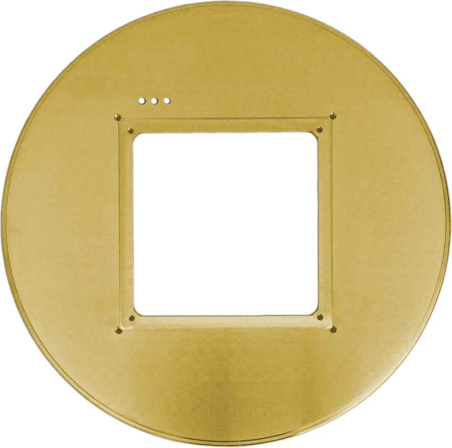
GND 25 | Gold-plated steel ground plane; 103 x 103 mm recess accepts GNDA 01-04 adapters and 100 x 100 mm TEM-cell boards. Height: 24 mm; Depth of the recess: 1.7 mm; Diameter: 218 mm; Opening: (103 x 103) mm; Weight: 2 kg |
Software, computer and control requirements
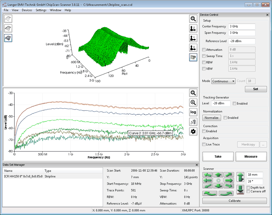
ChipScan-Scanner supports planar and volumetric field acquisition, visualization, processing and analysis, and image/data export. The full set includes the USB software license. Basic sets do not include ChipScan-Scanner. The separate Langer SDK supports custom positioning-control software on Windows and Linux; this does not mean the ChipScan-Scanner desktop application runs on Linux.
| Computer requirement | Published value |
|---|---|
| Operating system | Windows 11/10 64-bit (latest service packs) |
| Monitor resolution | (1280 x 1024) px |
| HD space | 1 GB |
| Processor | Intel Core i7 2.7 GHz |
| Memory | 8 GB |
| Graphics card | AMD Radeon 7950 |
| Graphics memory | 3 GB |
Download spectrum analyzer compatibility and interface guide (PDF). Model, interface, driver-test status, listed firmware and limitations are kept in this separate document. Confirm the software version, firmware and connection before ordering.
Scanner applications and positioning views
| View | Description |
|---|---|
 |
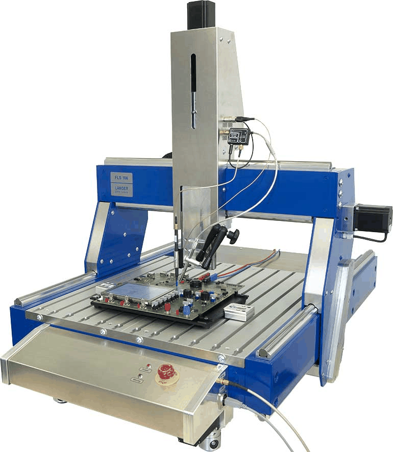
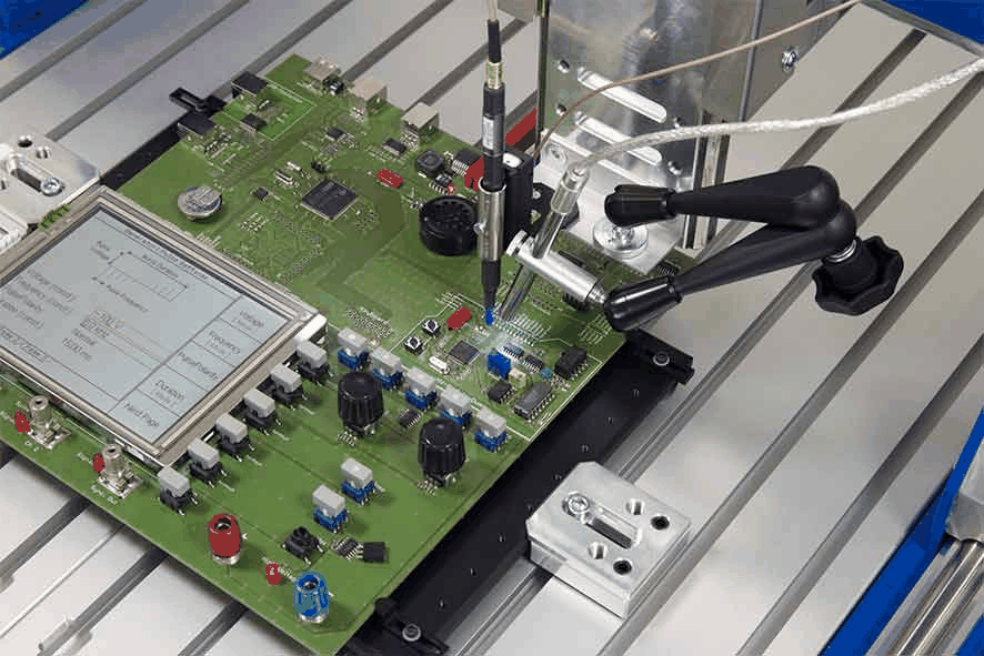
FLS 106 application with board, near-field probe and microscope camera |
 |
Application of FLS 106 with near-field probe and microscope camera on board to be tested |
Probe selection
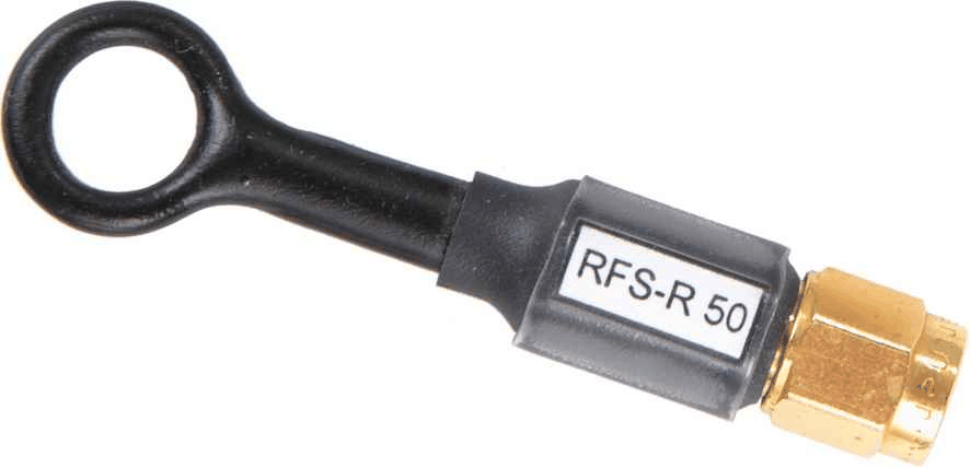
LFS, RFS and XFS passive scanner probes are available as configuration choices; verify the required holder, clearance and orientation. ICR microprobes and injection probes belong to separate product families and need their corresponding setup.
Scanner probe family comparison
| Family | Models | Coverage | Field types | Choose for |
|---|---|---|---|---|
 LFS |
1 | 100 kHz-50 MHz | H | Low-frequency switching-current and magnetic-field mapping. |
 RFS |
7 | 30 MHz-3 GHz | H and E | General PCB investigations with large-area and fine-resolution geometries. |
 XFS |
4 | 30 MHz-6 GHz | H and E | PCB near-field mapping when coverage above 3 GHz is needed. |
The passive scanner probes below have model-specific SMA connections and no power supply in their published specification. ICR near-field microprobes are a separate precision-probe class; use the existing ICR near-field microprobe range when micrometer-scale sensing is needed.
Datasheets and reference documents
| Product | Document |
|---|---|
| FLS 106 PCB set | FLS 106 PCB set - Datasheet |
| FLS 106 PCB basic set | FLS 106 PCB basic set - Datasheet |
| CS-Scanner | CS-Scanner - Datasheet |
| SH 01 | SH 01 - Datasheet |
| UH DUT | UH DUT - Datasheet |
| GND 25 | GND 25 - Datasheet |
Product videos
Compare before ordering
Open the complete scanner and scanner-probe comparison guide
Scanner comparison - differences that matter
| Scanner | Best fit / benefit | Travel and axes | Minimum step | Positioning speed | Weight / footprint |
|---|---|---|---|---|---|
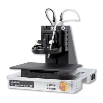 ICS 105 |
Compact IC workbench scanner Choose for a small IC scan area, finer minimum positioning increment and a compact bench footprint. |
50 x 50 x 50 mm; +/-180 deg | 10 um linear; 1 deg rotation | 10 / 10 / 5 mm/s; 90 deg/s | 23 kg; 350 x 400 x 420 mm |
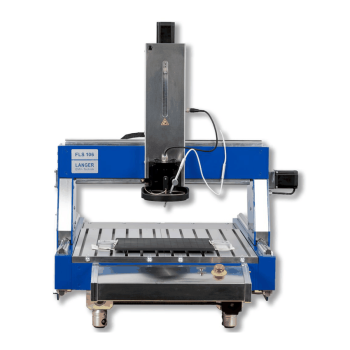 FLS 106 IC |
Large-area scanner with probe rotation Choose when the DUT or fixture needs a larger area and IC-style angular probe scans are important. |
400 x 600 x 120 mm; +/-180 deg | 20 um linear; 1 deg rotation | 20 / 25 / 10 mm/s; 90 deg/s | 75 kg; 1030 x 775 x 900 mm |
 FLS 106 PCB |
Large-area three-axis PCB scanner Choose for repeatable X/Y/Z scans over assemblies without the IC model's motorized alpha rotation. |
400 x 600 x 120 mm; no alpha axis | 20 um linear | 20 / 25 / 10 mm/s | 75 kg; 1030 x 775 x 900 mm |
Travel, step size and speed are listed in X/Y/Z order. Minimum positioning step is not probe spatial resolution, repeatability or positioning accuracy. Achievable field-map detail depends on probe size, spacing, orientation and the complete measurement chain. Scanner frequency coverage is determined by the selected probe and RF instrument, not the motion platform.
OTHER PRODUCTS IN THE SAME CATEGORY:


Langer FLS 106 IC | Large-area scanner with probe rotation
Langer FLS 106 PCB | Large-area three-axis PCB scanner
Langer Scanner and Scanner Probe Comparison Guide
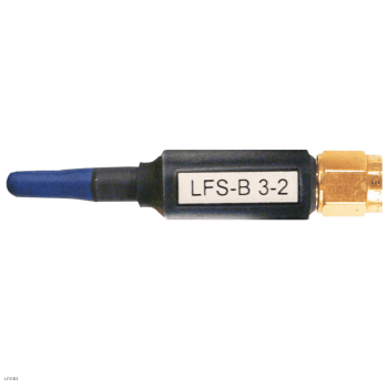
Langer LFS Scanner Probes | 100 kHz to 50 MHz
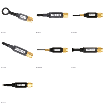
Langer RFS Scanner Probes | 30 MHz to 3 GHz
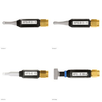
Langer XFS Scanner Probes | 30 MHz to 6 GHz
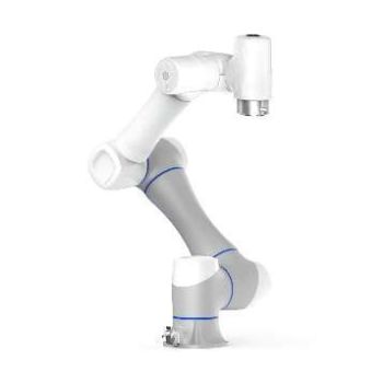
EMProbe CR5 - Custom Large-Reach Robotic EMI Scanning System
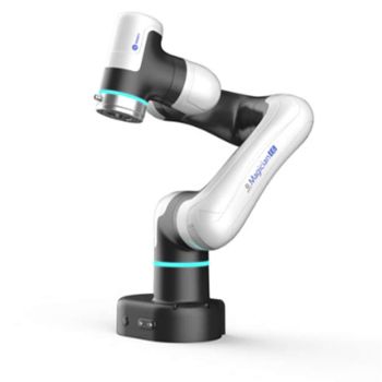
EMProbe-DBM-E6 — 6-Axis Robotic Near-Field EMI Diagnostics on the Bench
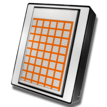
EMScanner+: 150 kHz- 6 GHz, w/ Real-Time Spectrum Analyzer, EMC desktop scanner
EMScannerR+: 150 kHz- 6 GHz, w/ Real-Time Spectrum Analyzer, EMC desktop scanner
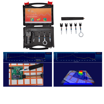
NFPKIT, EM Near Field Probe Kit w/Camera & Software
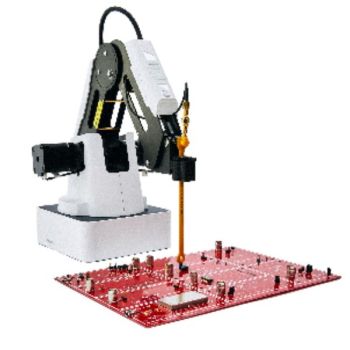
EMProbe: 9kHz- 18 GHz, 0.2mm resolution, EMC robotic scanner
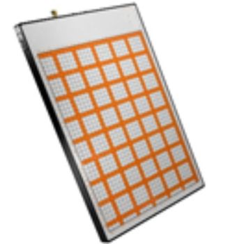
EMScanner: 150 kHz- 8 GHz, 3.5mm Resolution, EMC desktop scanner
EMScannerR: 150 kHz- 8 GHz, 0.06mm resolution, EMC desktop scanner
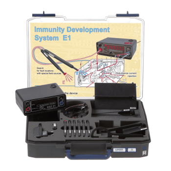
Langer E1 set | PCB Immunity Development System
Langer Scanner and Scanner Probe Comparison Guide
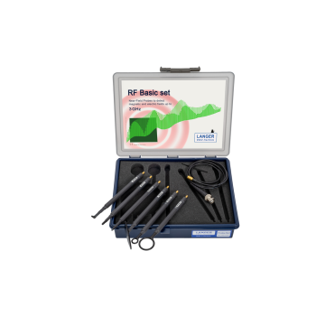
Langer Handheld Near-Field Probes Selection Guide
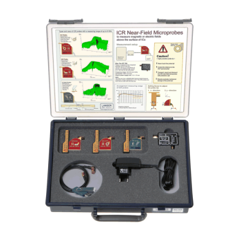
Langer ICR Near-Field Microprobe Selection Guide
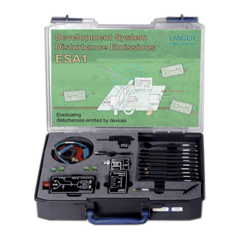
Langer ESA1 Set | EMC Emission Development System