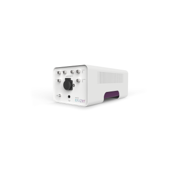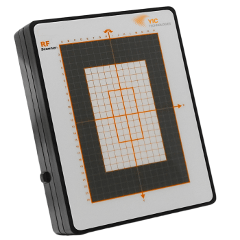

EMScannerR: 150 kHz- 8 GHz, 0.06mm resolution, EMC desktop scanner
- Capability:
-
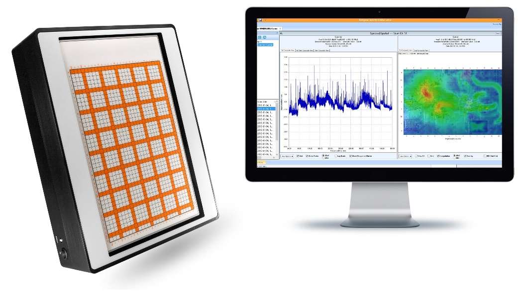
- Spectral scan, spatial scan, peak-hold, continuous scanning, spectral and spatial comparison, scripting, limit lines, report generation, and notes.
- Spatial scan time:
-
- Continuous real-time for the entire scan area (1,218 probes activated) when Level 1 is selected: 5 sec.
- Selected area 2.25 cm x 2.25 cm, 9 probes activated.
- Level 1:
- Spectral scan time:
-
- 11 seconds for L 10 cm x W 10 cm (L 4” x W 4”, 178 probes activated) from 10 MHz span to 110 MHz and 122 kHz RBW. Scanning area, span, and RBW are user-selectable within spectrum analyzer specifications
- Supported operating systems: Windows 10®
- Supported overlays: Picture in JPEG format
- Standard Gerber© RS274x format and HPGL form
PARTNER:
MARKETS:
CATEGORIES:
TEST STANDARDS:
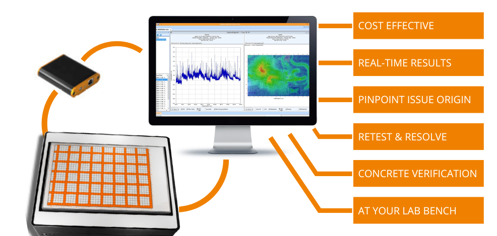
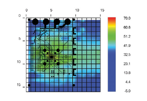
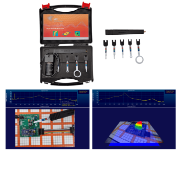
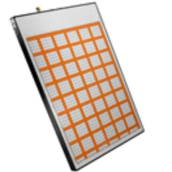
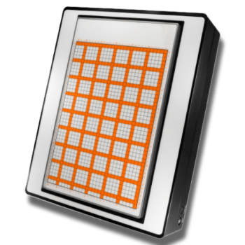
EMScannerR: 150 kHz- 8 GHz, Upto 0.06mm resolution, EMC desktop scannerThe world’s fastest EMC/EMI diagnostic system has been reinvented to assist high-density board designers in visualizing the root causes of potential EMC and EMI problems during pre- and post-EMC compliance testing. EMScannerR enables the PCB and design engineers to diagnose EMC/EMI problems between 150 kHz and 8 GHz. EMScannerR provides 8 levels of resolution (60 microns – 7.5 mm). EMScannerR provides 8 levels of resolution (60 microns – 7.5 mm). Level 1 resolution (7.5 mm) allows the engineers to visualize the hot spots, current loops, or intermittent problems in real time. After locating the unintended radiators, engineers can zoom into the problem by selecting the resolution level based on the density of the board design. EMScannerR provides unique pre- and post-EMC compliance testing that images emissions. Design engineers must find, characterize, and address unintended radiators or RF leakage during any new PCB development process to pass compliance testing. EMScannerR allows board designers to pre-test and resolve EMC and EMI problems early on, thus avoiding unexpected EMC compliance test results.
High-resolution EMC scanner Ideal PCB projects for EMScanner are boards designed for high speed, high power, and/or high density/complexity. Any PCB that places a premium on board real-estate also qualifies as an excellent candidate. The compact, flat scanner provides PCB design teams with an easy-to-use, costeffective, and proven tabletop solution. Emission, immunity, filtering, EMI shielding, broadband noise and Common Mode testing are some of the applications that the EMScanner system addresses in mere seconds. With EMScanner, design teams can personally test their designs without relying on another department, test engineer, or time-consuming off-site testing. After diagnosing even an intermittent problem, the engineer can implement a design change and retest, and the results provide concrete verification of the design change's effectiveness (or not). EMScanner diagnostic capabilities allow design teams to reduce testing time by more than two orders of magnitude. Users have also documented fifty percent reductions in design cycle times.
Available for Rent from our Rental Patern Advance Test Equipment Rentals (ATEC)Specifications
EMViewer Software
With the new & improved software, the following features are available: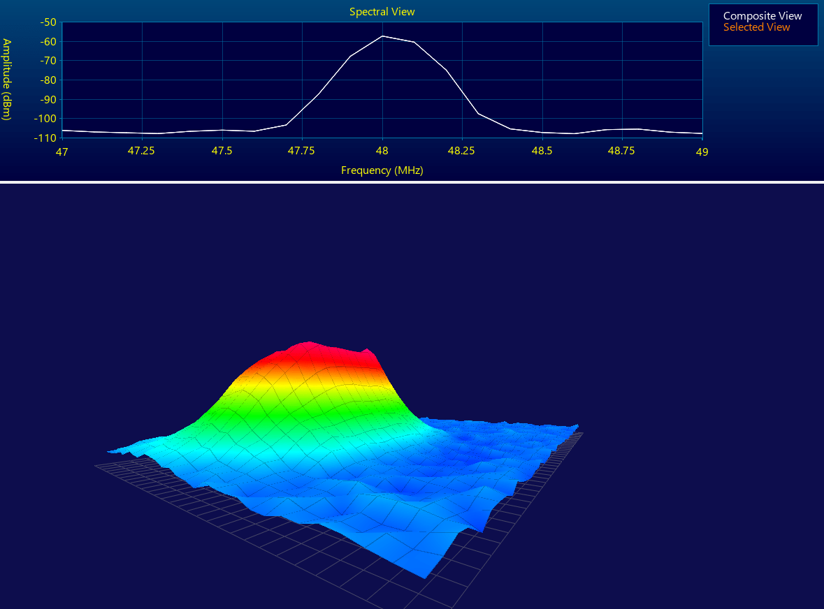
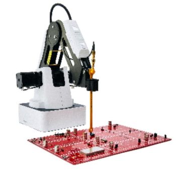
EMC scanning of mixed technology PCBs with Field Master and YIC high-resolution EMScanner |


