Diagnosing Board-Level EMC Design Issues with the EMScanner
Diagnosing Board-Level EMC Design Issues with the EMScanner
Abstract
The EMScanner is a powerful diagnostic instrument that provides PCB design teams with fast, high-resolution magnetic near-field data to detect electromagnetic compatibility (EMC) design issues. It delivers real-time spatial and spectral scan images, helping engineers to quickly identify and mitigate both constant and time-varying emission sources across a wide frequency range—from 150 kHz to 8 GHz. This article expands on core concepts with examples in filtering, shielding, common-mode interference, current flow, immunity, broadband noise, and additional use cases like NFC and GPS diagnostics. The EMScanner empowers engineers to perform fast, accurate EMC assessments during the design phase, avoiding costly late-stage compliance failures.
Target Audience: PCB designers, hardware engineers, and verification engineers, particularly those new to EMC principles.
1. Introduction
Modern PCBs—especially those that are compact, high-speed, or high-power—can be challenging to design for EMC compliance. Even the best-laid circuits may emit or pick up unwanted RF energy, which could lead to compliance failures.
The EMScanner helps bridge the gap between design and compliance testing by imaging electromagnetic emissions directly from the PCB surface in real time. These emissions, which result from parasitic currents, poor layout, or insufficient shielding, can be diagnosed and mitigated early. Because the system provides rapid visual feedback, it enables iterative debugging during design—long before sending a board to the EMC chamber.
Instead of waiting days for lab results, teams can make changes and retest instantly, using the EMScanner on their lab bench. It even allows visualization of intermittent emissions and provides clear validation of mitigation measures. Many teams have reported design cycle time reductions of over 50%.
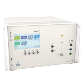
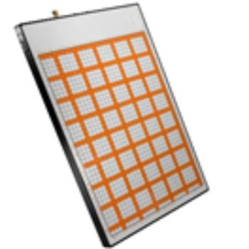
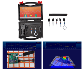
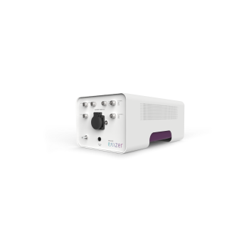
2. System Description
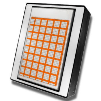
The EMScanner consists of:
-
A patented scanner base with 1,218 H-field magnetic probes (2,436 loops) spaced every 7.5 mm.
-
An external spectrum analyzer for frequency domain measurement.
-
A PC running EMViewer software for real-time display.
This probe array forms an electronically switched grid capable of 3.75 mm resolution and works across 150 kHz to 8 GHz.
The system is small enough for any workbench and requires only standard accessories. It offers fast and intuitive spatial imaging without the need for complex chamber environments.
3. Filtering: Real-Time Validation
Objective: Quickly identify the effectiveness of filters on emission sources.
Miniaturization has made it more difficult to manage signal and power integrity. During development, emissions can originate from voltage regulators, clock lines, or switching nodes. The EMScanner can pinpoint these sources and allow designers to test mitigation strategies such as:
-
Inserting ferrite beads
-
Implementing common-mode chokes
-
Replacing or relocating capacitors
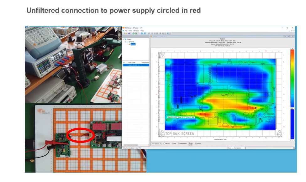
Case Study: A satellite receiver board was tested before and after adding a filter to the power cable. Figures 1–2 show the DUT’s emissions before filtering, the added filter location, and the resulting suppression of emissions post-filtering.
4. Shielding: See the Impact Instantly
Objective: Validate the effectiveness of shielded components or enclosures.
Shielding is an important tactic to reduce emissions, especially for clock generators or RF subsystems. The EMScanner's spatial scanning allows engineers to:
-
Locate emissions from unshielded components
-
Overlay post-shielding results for comparison
Figures show spatial scans with and without shielding applied to the same DUT. The EMScanner’s visual difference between the two states confirms the effectiveness of the shielding solution.
DUT with shielding showing results of a Spatial Scan.

DUT without shielding showing results of a Spatial Scan.
5. Common Mode Currents: Hidden Trouble
Objective: Identify and mitigate emissions originating from common-mode coupling.
Common-mode currents are especially problematic because they travel along cables and can radiate far-field energy, causing failures even in well-grounded systems. EMScanner helps:
-
Visualize noise coupling onto cables and connectors
-
Trace the source back to PCB return paths or poor decoupling
The included image shows coupling into a connector—highlighting a frequent EMC failure cause.
EMScanner spatial scan showing low level noise coupling onto a connector at the top Left.
6. Current Distributions: Visualizing the Real Flow
Objective: Visualize changes in current paths caused by component layout and placement.
By examining loop areas and current paths, engineers can observe how:
-
Routing impacts loop emissions
-
Bypass capacitor placement affects noise levels
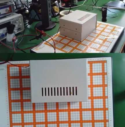
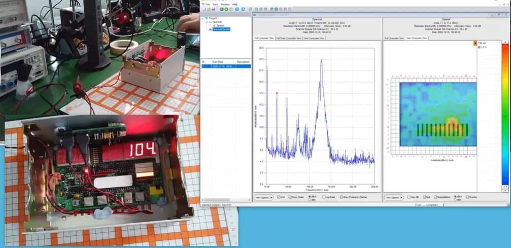
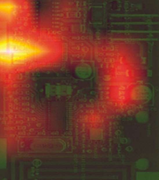
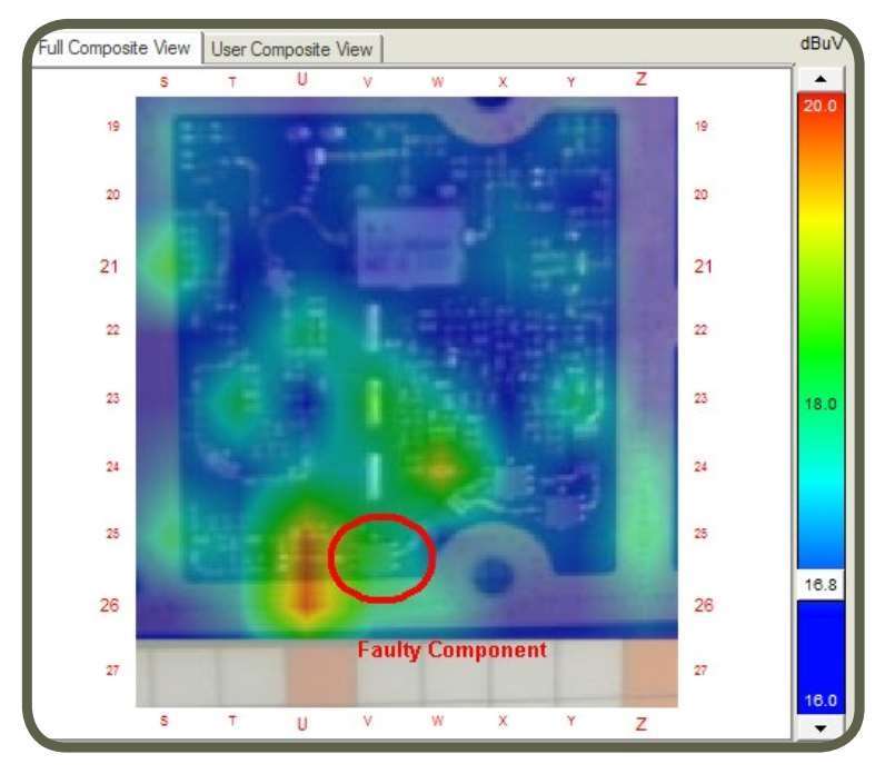
Case Study: A taximeter PCB emitted significant energy at 11.06 MHz. After adding a decoupling capacitor, emissions dropped by 8 dBµV. The EMScanner scan clearly shows the visual difference.
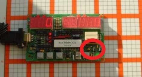
Taximeter PCB positioned on the patented scanner and tested at 11.06 MHz. The
test measures noise without and then with a capacitor added (location in red circle)
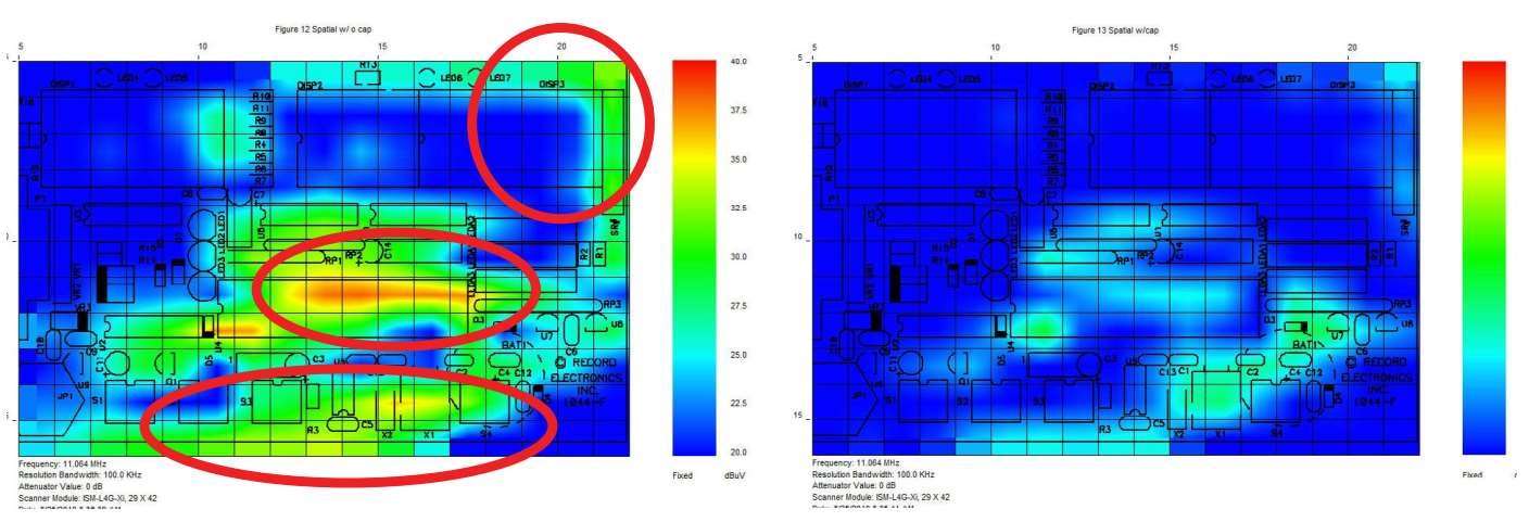
Left: Taximeter PCB test with no capacitor – noise capacitor reduces circled in red
Right: Taximeter PCB test with Noise by at least 8 dBuV
7. Conducted Immunity: Diagnose Susceptibility
Objective: Map how injected RF current flows through a board during conducted immunity testing.
Conducted immunity failures are difficult to isolate. Using RF injection, the EMScanner reveals:
-
Where the signal enters
-
Which components are affected
-
How mitigation like shielding or grounding, helps
Figures demonstrate board scans with and without injected RF at 50 MHz, showing the areas most impacted.
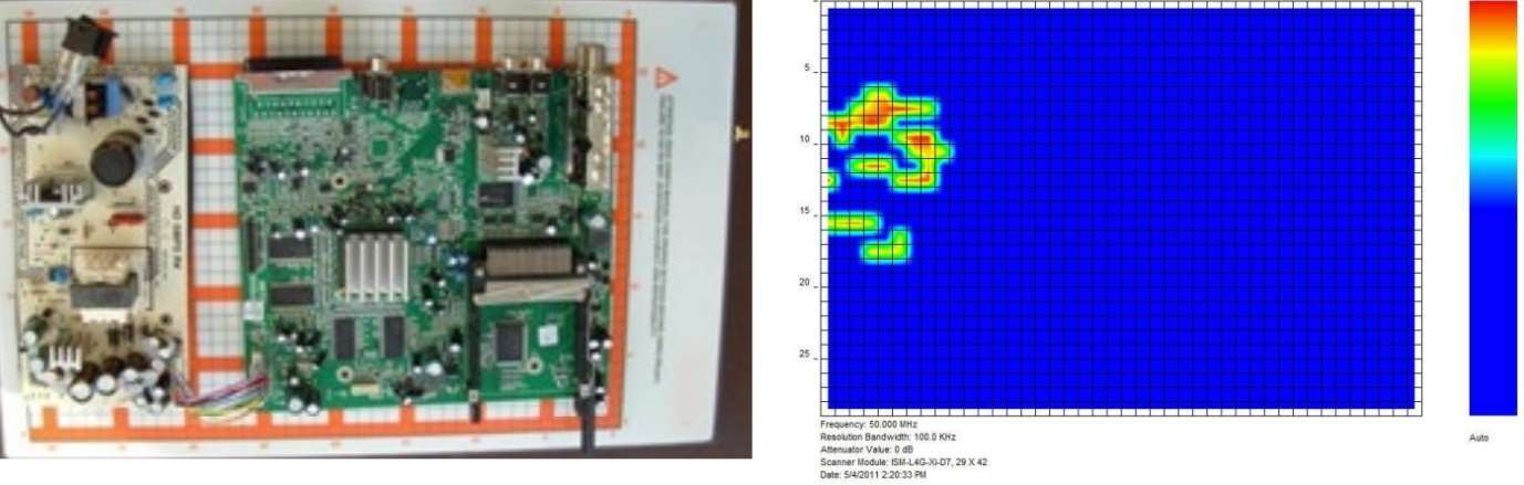
EMScanner spatial scan at 50MHz with no noise injection.
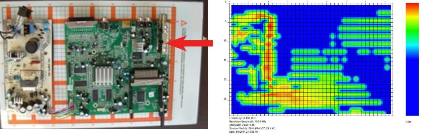
EMScanner spatial scan at 50MHz with noise injection at right edge of board.
8. Emissions Along Traces: Zooming In
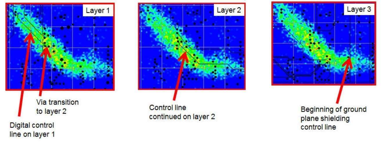
Objective: Localize emissions down to individual traces and vias.
With high spatial resolution, the EMScanner enables:
-
Zooming in on hotspots
-
Tracing emissions across layers
A trace between an MCU and crystal was isolated as a key noise path using EMScanner. After modifying the return path, emissions were resolved.
Spatial Scan results of the PCB by EMScannerR
Left: Run a real-time spatial scan to see the emissions on the whole board.
Right: Then zoom into the problem area for further analysis.
9. Broadband Noise: Mapping SMPS Emissions
Objective: Identify the source and evolution of broadband switching noise.
Switched-mode power supplies (SMPS) generate broadband emissions. The EMScanner can:
-
Sweep across frequency bands
-
Use the limit line feature to quickly determine out-of-spec behavior
-
Guide placement of snubbers, beads, or layout changes
As an example, a Switched Mode Power Supply (SMPS) can cause broadband noise in control electronics, other components, and the PCB itself. To characterize such emissions, EMScanner quickly scans the board across a broad frequency range. The user can then select and characterize specific frequencies to observe how the noise evolves spatially across the frequency range. This allows the design team to map the noise, confirm its source, and implement appropriate mitigation. The software’s limit line feature serves as a key descriptor and allows project engineer(s) to distribute this test to less-experienced technicians.
Spectral scan of the broadband noise from a power supply
10. NFC Antenna Testing: Performance Verification
Objective: Ensure proper operation of near-field communication antennas.
For NFC, far-field patterns are not useful. The EMScanner offers:
-
Burst mode detection
-
Peak hold visualization
-
Fast overlay comparison with antenna design
Considering the size, frequency and distance, antenna radiation pattern is not a meaningful parameter for NFC designers. Amplitude and distribution of the signal are important. The EMScanner is a fast and effective tool that measure and displays the emissions from an NFC antenna using very-near-field technology. The peak-hold mode of the EMScanner can still create a full image of the antenna’s emission in
seconds even with a burst NFC signal. These results allow a designer or a tester to verify that the antenna is operating as expected and to validate the antenna’s emission level versus calculated specifications.
In the example below a phone has a back case which comes off and exposes every antenna used for GSM, Wi-Fi, NFC etc. The NFC antenna section is highlighted in red. The results from the near-field scan show strong currents in an area similar to the shape of the highlighted antenna (right image below).
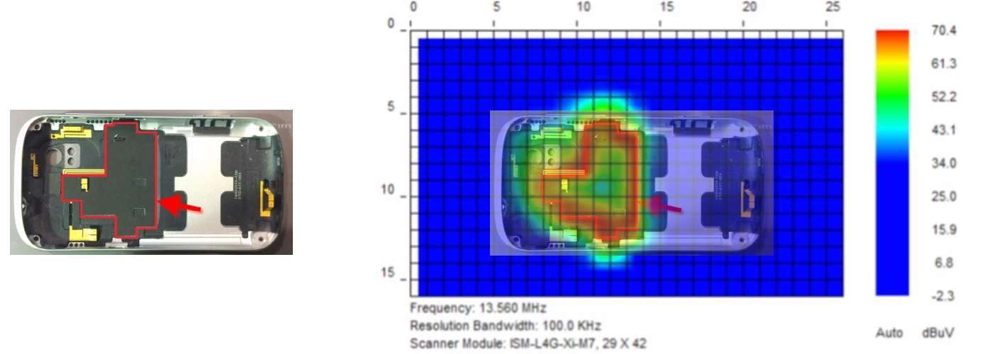
Spatial Scan of the smart phone at 13.560 MHz
When the very-near-field result is overlaid on top of the photograph of the phone case itself, the image clearly shows the strong correlation between the NFC antenna emissions and the antenna’s physical location.
11. GPS Self-Interference: Debugging Coexistence Issues
Objective: Diagnose internal interference with sensitive GPS receivers.
A common problem is digital circuitry interfering with sensitive analog/RF receivers. In this example:
-
Turning on the camera introduced strong emissions in the GPS band
-
Emissions were traced through SDRAM coupling into the radio chipset
Spatial and spectral scans isolated the problem and informed shielding strategies.
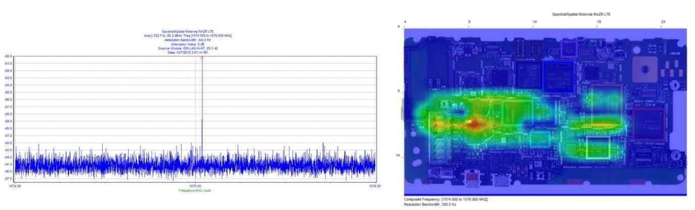
Spectral Scan (left) and Spatial Scan (right) of the mobile phone.
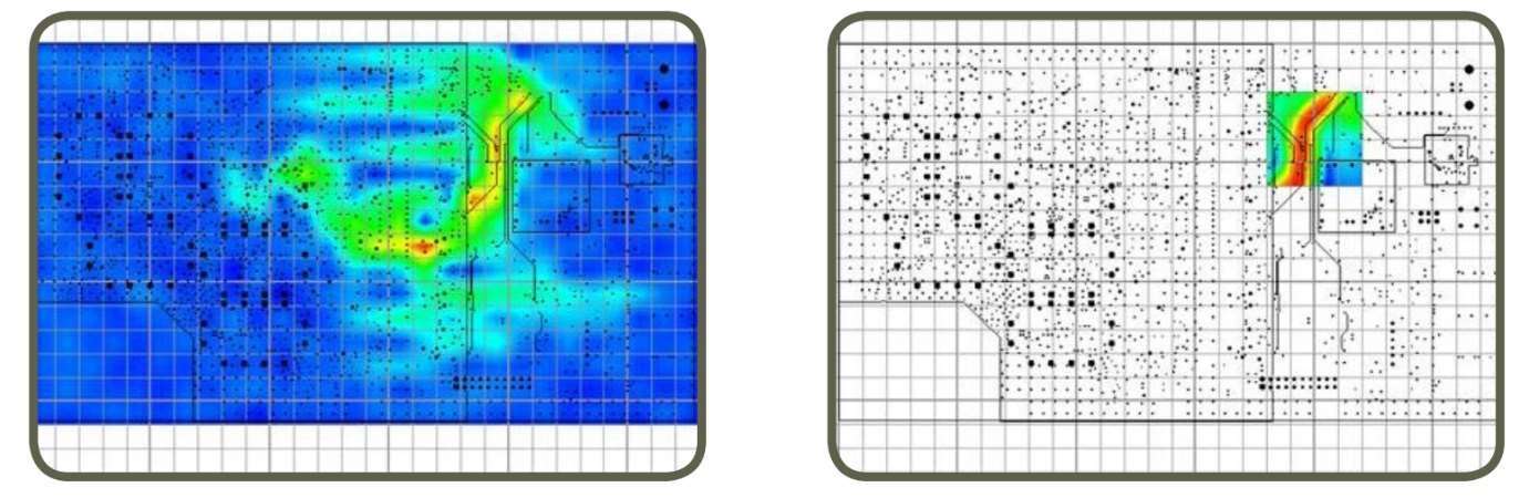
12. Manufacturing Problem Troubleshooting: Golden Sample Comparison
Objective: Detect assembly defects and inconsistencies.
Comparing “golden” (known-good) boards to faulty units allows manufacturers to:
-
Detect misplaced or rotated parts
-
Identify cold solder joints
Tests were done at a manufacturing facility in Europe to determine if problems could be identified when comparing the very-near-field emissions of good boards and problem boards. There was an issue that had been eluding detection; it showed as a poor RSSI reading and had been isolated to the IF chain. An EMxpert spatial scan comparison of the IF currents between a good board and the problem board indicated an issue at a location different from where the manufacturer had assumed the problem was. Further investigation uncovered a soldering issue with a single component. A scan of the entire board at the IF frequency clearly showed a difference in the spatial profile.
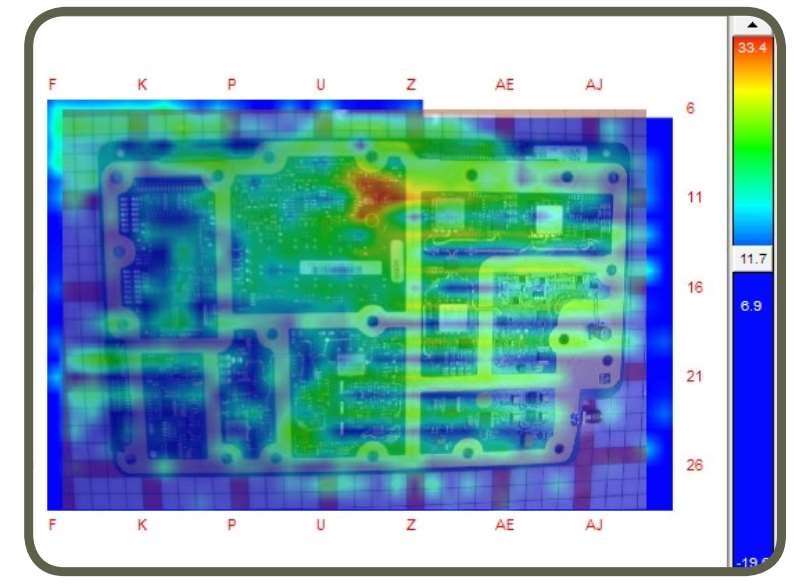
Spatial Scan of the Good Board at the IF frequency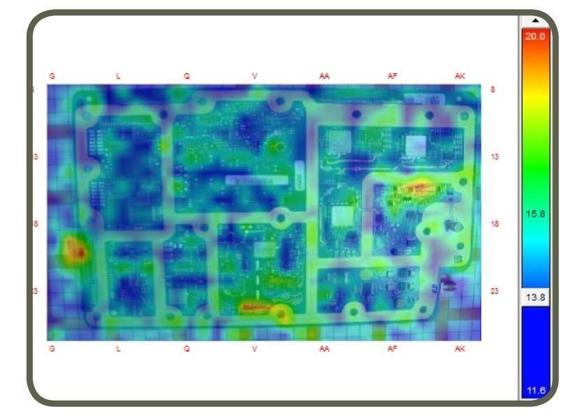 Spatial Scan of the Good Board at the IF frequency
Once it was confirmed that there was a problem at the IF frequency a focused
analysis on the IF chain was done. Zooming in on the area of the IF right as it exited
the first mixer showed a very-near-field variation immediately after the SAW filters.
Spatial Scan of the IF Chain of the Good Board Showing Strong Emissions
Throughout
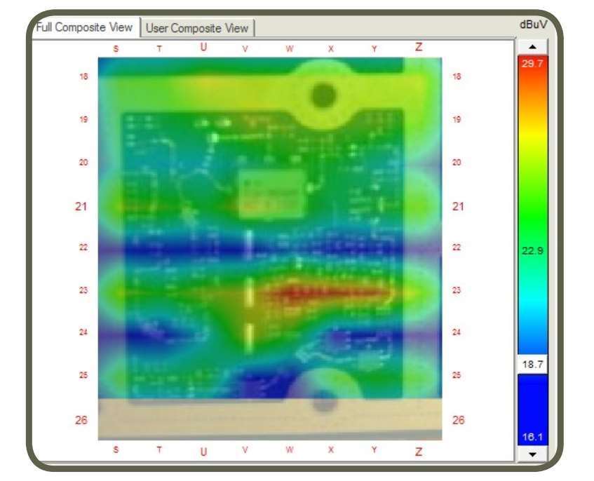
Spatial Scan of the Bad Board at the IF Frequency
After viewing the large variation in the very-near-field emissions at this location, a visual inspection of the board revealed the SAW filter highlighted in the image above was populated with a 90° rotation meaning no signal would pass through.
13. Summary
The EMScanner offers a powerful and immediate method for diagnosing emissions and coupling issues at the board level. It helps reduce:
-
Debugging time
-
Design iterations
-
Costly failures at compliance labs
With real-time spatial scans and support for multiple engineering workflows, the EMScanner is an essential tool for every serious PCB design team and an invaluable teaching aid for understanding EMC in practice.
Educational Tip: Try comparing two board layouts—one compliant and one not—and observe how small layout changes produce dramatic emission differences.
For technical specifications and real-world demos, visit:
???? https://absolute-emc.com/product/emscanner
???? https://yictechnologies.com